
1. Causes of Film Deformation and Solutions:
Causes:
(1) Failure to control temperature and humidity
(2) Excessive temperature rise in the exposure machine
Solutions:
(1) Typically, temperature should be controlled at 22 ± 2°C, and humidity should be maintained at 55% ± 5% RH.
(2) Use cold light sources or exposure machines with cooling systems, and regularly change backup films.
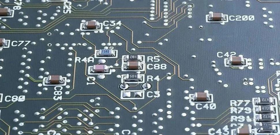
At PCBYES, we understand the importance of maintaining optimal environmental conditions in PCB fabrication. With over 5 years of experience in the PCB industry, we ensure the proper control of temperature and humidity throughout the manufacturing process to minimize risks like film deformation.
2. Process Methods for Correcting Film Deformation:
Hole Position Adjustment Method ("Hole Position Change Method"):
If the operation of a digital programming device is mastered, the film can first be aligned with a drill test board, and the deformation in the length and width can be measured. The hole positions can be adjusted by elongating or shortening them according to the deformation values. The deformed film is then matched with the modified test board, eliminating the complex task of cutting and splicing films, and ensuring the integrity and accuracy of the patterns.
Hanging Method ("Air Hanging Method"):
This method targets the physical changes in the film caused by varying environmental temperature and humidity. Before copying the film, it is removed from its sealed bag and hung in the work environment for 4-8 hours. This pre-deformation ensures that the copied film has minimal deformation, reducing distortion during the copying process.
Splicing Method ("Splicing Method"):
For simple circuit designs with larger line widths and spacing, or when the deformation is irregular, the deformed section of the film can be cut and matched with the hole positions on a drill test board. After splicing, the film can be copied. This method is effective for larger or irregular deformations, where re-alignment is necessary.
Pad Overlap Method ("Pad Overlap Method"):
In this method, enlarged pads cover the distorted lines on the film, ensuring that the minimum ring width requirement is met. The enlarged pads help correct the deformation in the circuit pattern, improving the overall alignment.
Layout Adjustment Method ("Paste Layout Method"):
The deformed pattern on the film is scaled up, and a new layout is prepared for the film. This method ensures that the corrected film can maintain proper alignment when transferred to the PCB.
Photographic Method ("Photographic Method"):
In this method, the deformed film pattern is enlarged or reduced using a camera, ensuring that the film's visual representation matches the required specifications.
3. Considerations for Related Methods:
► Splicing Method:
Applicable to: Films with less dense lines and inconsistent deformation across layers, especially for solder mask films and multi-layer PCB films for power and ground planes.
Not applicable to: Films with high-density traces or with line widths and spacings less than 0.2 mm.
Precautions: When splicing, care must be taken to avoid damaging the traces or pads. After the splice, attention should be paid to ensuring that the connections are correct when reworking the layout.
► Hole Position Adjustment Method:
Applicable to: Films with consistent deformation across layers. Even films with dense traces are suitable for this method.
Not applicable to: Films with uneven deformation, especially those with significant localized distortion.
Precautions: After elongating or shortening the hole positions, any out-of-spec holes must be redefined and set correctly on the programming device.
► Hanging Method:
Applicable to: Films that have not yet been deformed and films that need to be prevented from deforming after copying.
Not applicable to: Films that have already undergone deformation.
Precautions: The films should be hung in a ventilated and dark environment (with safety precautions if necessary). Ensure the temperature and humidity of the hanging environment match the working conditions.
► Pad Overlap Method:
Applicable to: Films with less dense traces and line widths and spacings larger than 0.30 mm.
Not applicable to: Films that require strict visual appearance specifications.
Precautions: Since overlapping pads can lead to an elliptical shape, there may be a light halo around the edges of the pads and lines after copying, causing some distortion in the final result.
► Photographic Method:
Applicable to: Films with consistent deformation in both length and width. This method is also suitable for silver halide films when modifying drill test boards is difficult.
Not applicable to: Films with inconsistent deformation in the length and width directions.
Precautions: Accurate focusing is crucial during the photographic process to avoid distortion of the lines. The film may experience significant losses, and multiple adjustments are often needed to achieve a satisfactory result.
At PCBYES, we are committed to offering high-quality PCB fabrication and prototype services to meet a wide range of needs. Our expertise in providing PCBA turnkey services ensures that you receive the best in quality, reliability, and efficiency, and we address issues like film deformation with careful attention to detail. From temperature and humidity control to advanced correction techniques, we strive to offer optimal solutions for all your PCB manufacturing requirements.
Deformation in PCB films can be caused by several factors, including poor temperature and humidity control and high exposure to machine temperatures. There are various methods for correcting this issue, such as adjusting hole positions, pre-deforming films through hanging, splicing sections, using enlarged pads, or photographic techniques. Each method has its applicable scenarios, advantages, and limitations. When applying these correction techniques, attention to detail is essential to maintain the integrity and accuracy of the PCB design and to prevent further damage to the film.


